
Caption
|
Experimental studies of light-matter interactions inside on-chip waveguides containing mesoscopic ensembles of quantum emitters:
Compared to single quantum emitters, ensembles of quantum emitters can frequently offer significant advantages for implementing controllable single photon interactions. These advantages include collective enhancement of light-matter interaction, robustness to noise and decoherence, and the inherent ability handle light pulses containing multiple photons. We plan to engineer and explore new QED effects with ensembles of atoms inside on-chip hollow waveguides and ensembles of solid state emitters embedded in photonic-crystal waveguides. Moving from the fiber-based geometries, such as the tapered-fiber and photonic-crystal fiber, to an on-chip geometry will open new possibilities for control over the design of the photonic environment, scalability of these systems, and uses of recently demonstrated quantum optics phenomena, such as vacuum-induced transparency (VIT). We intend to combine these systems with slow light and light storage techniques and use them as platforms for quantum non-destruction (QND) measurements of photon states and photon number detection, as well as for quantum simulations of condensed matter phenomena. |
|
Development of integrated high-speed optical devices, scalable architectures, and integrated sensors based on atoms coupled to nano-scale photonic structures:
Atoms are generally considered too slow to be used as nonlinear medium in practical devices. However, photonic-crystal cavities can achieve Purcell regime or even strong coupling regime when coupled to atoms even for very modest Q-factors due to the extremely small mode volume of these cavities. This leads to the rise of a device capable of performing over a large bandwidth of frequencies (~GHz) and removes the drawback presented by the natural linewidth (~MHz) of optically accessible atomic transitions. This in turn would make an atom-based device fast enough to be competitive with solid-state devices. Thanks to the small footprint of the photonic-crystal cavities and all the atoms being inherently identical, this hybrid device should be scalable into a multi-device on-chip architecture for both quantum and classical information processing. Lastly, as this platform can be compatible with electronic devices and manufacturing, one can easily envision development of integrated atom-cavity based sensors for precision measurements. Moreover, as technological challenges become resolved, new applications for such devices will likely emerge. |

Caption
|
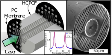
Fabry-Pérot Cavity Formed with Photonic Crystal Mirrors in a Hollow-Core Fiber
The purpose of our research is to create an optical resonator based on a hollow core photonic crystal fiber (HCPCF) in order to confine light around an atomic ensemble. We demonstrate this fiber-integrated Fabry-Pérot cavity by attaching a pair of dielectric metasurfaces to the ends of a HCPCF segment. The metasurfaces consist of perforated membranes designed as photonic-crystal slabs that act as planar mirrors but can potentially allow injection of gases through their holes into the hollow core of the fiber. Such a platform may allow for the enhancement of light-matter interactions that lead to nonlinearities in which effective photon-photon interactions may occur. Applications to these cavity devices include single photon all-optical transistors (shown below), cross-phase modulation, superradiant lasers, as well fundamental studies of quantum information and condensed matter systems.
The purpose of our research is to create an optical resonator based on a hollow core photonic crystal fiber (HCPCF) in order to confine light around an atomic ensemble. We demonstrate this fiber-integrated Fabry-Pérot cavity by attaching a pair of dielectric metasurfaces to the ends of a HCPCF segment. The metasurfaces consist of perforated membranes designed as photonic-crystal slabs that act as planar mirrors but can potentially allow injection of gases through their holes into the hollow core of the fiber. Such a platform may allow for the enhancement of light-matter interactions that lead to nonlinearities in which effective photon-photon interactions may occur. Applications to these cavity devices include single photon all-optical transistors (shown below), cross-phase modulation, superradiant lasers, as well fundamental studies of quantum information and condensed matter systems.
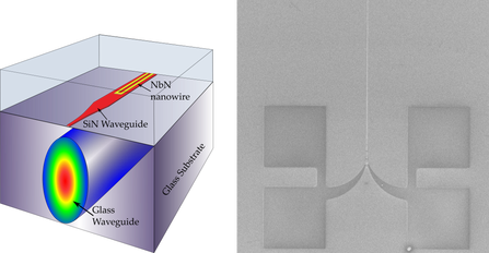
Integrated Superconducting nanowire single photon detector (SNSPD)
This project is devoted to design and fabricate a Superconducting nanowire single photon detector (SNSPD) evanescently coupled to silica waveguides including fibers or laser written waveguides. The device is expected to have high overall system efficiency compared to SNSPDs evanescently coupled to Si waveguides. NbN nanowire with width ~100 nm and thickness ~6 nm is being used as the detector. The feature is formed by reactive ion etching of an evaporated NbN film with HSQ-PMMA mask defined through Raith150 Two e-beam lithography.
This project is devoted to design and fabricate a Superconducting nanowire single photon detector (SNSPD) evanescently coupled to silica waveguides including fibers or laser written waveguides. The device is expected to have high overall system efficiency compared to SNSPDs evanescently coupled to Si waveguides. NbN nanowire with width ~100 nm and thickness ~6 nm is being used as the detector. The feature is formed by reactive ion etching of an evaporated NbN film with HSQ-PMMA mask defined through Raith150 Two e-beam lithography.
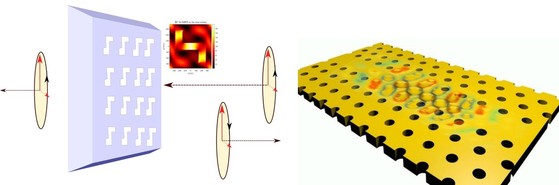
Automated Topology Optimization In Nano-scale Photonics and Flat Optics
Inspired by the widespread automated electronic design packages, the group is trying to build an automated photonics design tool mostly applicable to flat optics, meta-surfaces and photonic crystals. We combine various advanced optimization techniques including global stochastic methods together with local inverse techniques to design viable and robust nanophotonic structures surpassing the state-of-the-art topologies and immune to fabrication tolerances. The structures are intended to ultimately serve in flat-optics, chiral mediums, cavity QED and novel topologies for enhancing light-matter interactions.
Inspired by the widespread automated electronic design packages, the group is trying to build an automated photonics design tool mostly applicable to flat optics, meta-surfaces and photonic crystals. We combine various advanced optimization techniques including global stochastic methods together with local inverse techniques to design viable and robust nanophotonic structures surpassing the state-of-the-art topologies and immune to fabrication tolerances. The structures are intended to ultimately serve in flat-optics, chiral mediums, cavity QED and novel topologies for enhancing light-matter interactions.
TRISPEC: Arduino-controlled triple-grating high-resolution imaging spectrometer
Utilizing the Czerny-Turner design, we aim to build a low-cost high-resolution spectrometer that contains three diffraction gratings with increasing groove number. The triple-grating design facilitates the spectroscopic analysis processes. It is analogous to the multiple-objective design on a microscope. By switching between the different gratings, we may navigate quickly in the spectral domain using the weakest grating, and analyze the minute details in regions of interest using the strongest grating. As the grating is rotated to navigate in the spectral domain, the double-axes grating mounting scheme allows the grating surface to remain at the focal point of the focusing mirror. It not only reduces the effect of astigmatism, but also provides a greater effective area, allowing the spectrometer to explore a wider range of wavelengths. The grating orientation is measured with an optical absolute encoder. The encoder position improves the accuracy of the wavelength readings of the spectra and the user experience. To improve the spectral resolution of this spectrometer, we upscaled the distance and dimensions of all the crucial optical elements. This not only allows the diffracted lights to be further apart, but also decreases the effect of astigmatism. We mount the gratings on a repurposed grating turret originally from a 20cm triple-grating spectrometer from Princeton Instrument® and use an affordable (~$1,000) astronomy CMOS camera with a one inch sensor. We implement the control software using MatLAB. The spectrometer may also be used as a monochromator, which was used to filter quantum dot emissions.
Utilizing the Czerny-Turner design, we aim to build a low-cost high-resolution spectrometer that contains three diffraction gratings with increasing groove number. The triple-grating design facilitates the spectroscopic analysis processes. It is analogous to the multiple-objective design on a microscope. By switching between the different gratings, we may navigate quickly in the spectral domain using the weakest grating, and analyze the minute details in regions of interest using the strongest grating. As the grating is rotated to navigate in the spectral domain, the double-axes grating mounting scheme allows the grating surface to remain at the focal point of the focusing mirror. It not only reduces the effect of astigmatism, but also provides a greater effective area, allowing the spectrometer to explore a wider range of wavelengths. The grating orientation is measured with an optical absolute encoder. The encoder position improves the accuracy of the wavelength readings of the spectra and the user experience. To improve the spectral resolution of this spectrometer, we upscaled the distance and dimensions of all the crucial optical elements. This not only allows the diffracted lights to be further apart, but also decreases the effect of astigmatism. We mount the gratings on a repurposed grating turret originally from a 20cm triple-grating spectrometer from Princeton Instrument® and use an affordable (~$1,000) astronomy CMOS camera with a one inch sensor. We implement the control software using MatLAB. The spectrometer may also be used as a monochromator, which was used to filter quantum dot emissions.
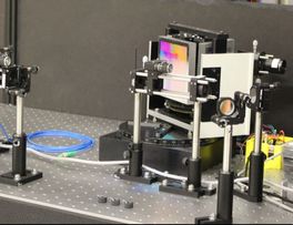
The triple grating turret mounted on a rotary stage.
|
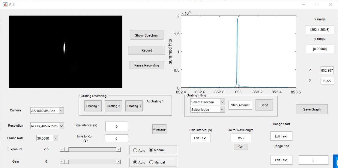
The graphical interface design of TRISPEC
|
